
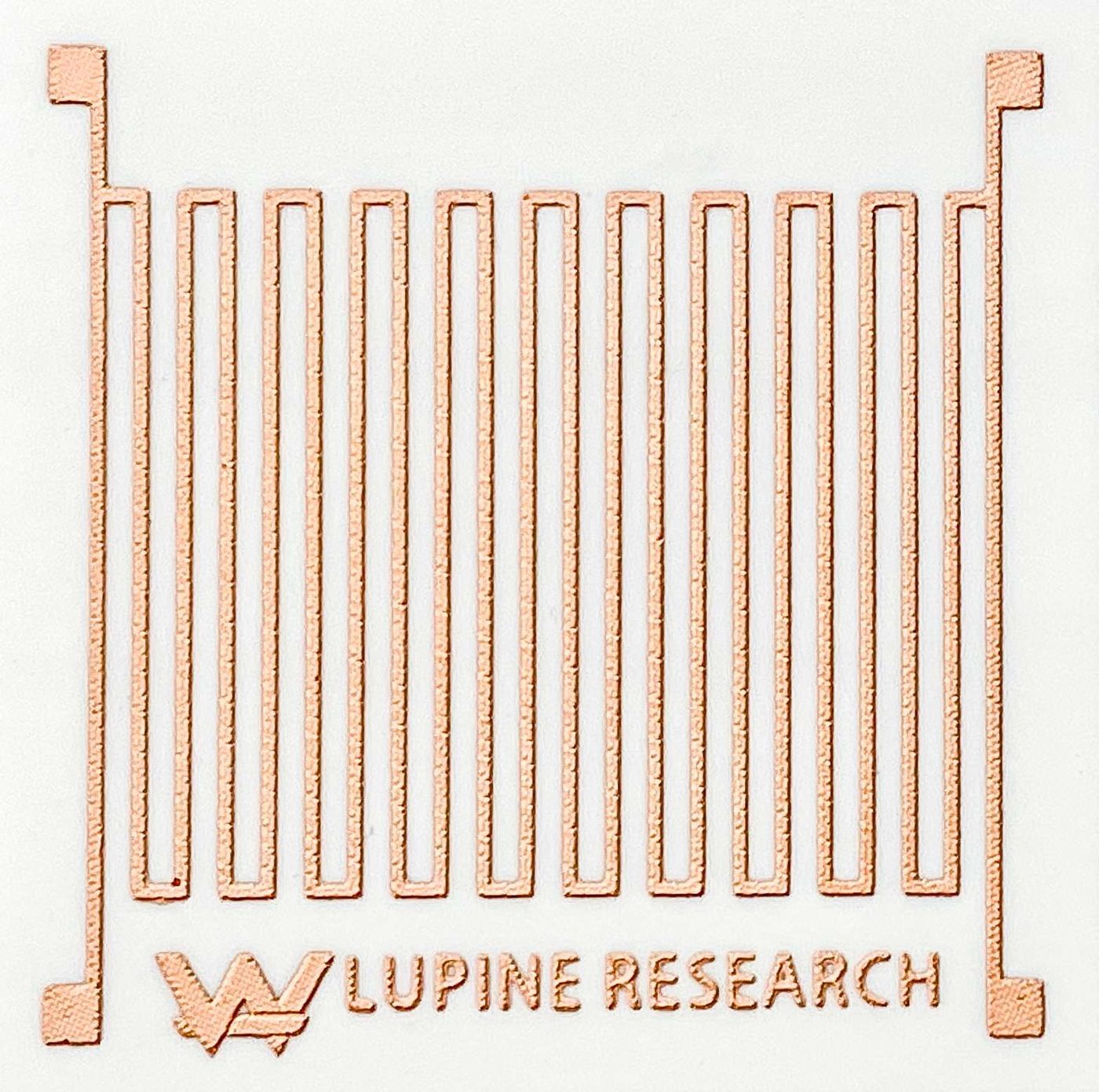
Thick-film screen printing deposits durable, functional layers of material onto substrates using patterned mesh screens. Conductive, resistive, or insulating pastes are printed and then fired at high temperature to create robust electronic components — high-quality results at economical prices.
The Process
- Substrate preparation — ceramic or polymer surfaces are cleaned for proper paste adhesion
- Screen printing — a fine mesh screen with patterned openings transfers paste to the substrate via squeegee
- Drying — solvents are removed to solidify the printed pattern
- Firing/sintering — high temperatures in a controlled atmosphere burn out the organic binder and sinter the metal particles
- Inspection — uniformity, conductivity, and adhesion are verified before finishing
Applications
- Printed circuit components and hybrid circuits
- Sensors and heaters
- Solar cells
- Conductive traces for high-power and high-frequency electronics
Advantages
- Highly cost-effective, from prototypes through production
- Supports a wide range of functional pastes and substrates
- Robust electrical and mechanical performance